close

Technology News

Technology News

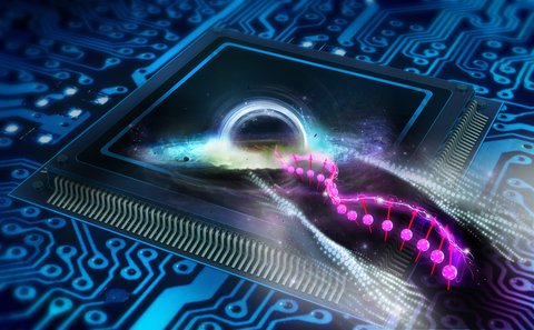
Black Holes on an Electronic Chip

Black Holes on an Electronic Chip

We Can Open Black Holes On An Electronic Chip, Scary?

The technological advancement stems from the need as the innovativeness of the inventors. Sometime people stumble upon great discovery when they are working on something completely different. A professor has taken the world by surprise by proposing a way which will lead to stimulation of black holes right on an electronic chip. So far we are not able to develop black on the earth in order to boost our study and knowledge about these.

This professor named Rembert Duine has worked together colleagues all the way from Chile to publish the underlying research in the Physical Preview Letters. Theoretically speaking all the right ingredients which are required to summon a black hole is present in the modern scientific labs. Scientists will be able to generate black within a time-span of two or more years from now to create black-holes in lab conditions.

No More Looking Into The Space For Black holes

The event horizon problem associated with the black hole in the space makes them extremely difficult to study. First of all they are dense which ensures that nothing escapes its gravitational pull once anything enters into its no return point. Researchers have made some progress in dealing with the problem associated with the event horizon phenomenon when they develop the same in the lab conditions. They were able to create such of no return which specifically deals with the spin waves and even helps in navigating through the fluctuations that are found in the magnetic materials.

A lot of science into action to make this theory works which includes the simple knowledge that the once we pass the electric current through the material then the electrons tends to drag the waves along with it. Like if we make use of a wires which is think at one end and thin at another and the when we pass the electricity then the electrons are likely to flow faster on thin end.

Points of no return have never been investigated in the electronic chips and they are less likely to originate as well. Therefore opting for chips to build the black holes appears as the right and sensible choice though currently in theory. Secondly having black holes on the chips will help in studying the effects of Hawking radiation in higher temperatures with quite ease and grace.

The Quantum Computers

The hawking radiation is caused by the particles which remain in pair and they happen to be quantum mechanically entangled. Researchers have proposed that they will be making use of the entanglement found in the electronic devices in order to create black holes right on the chip in upcoming days. In the quantum computers and even the quantum technologies the entanglement acts as the key ingredient and scientists has found right way to work for their own advantage. Creating black holes on chips will allow them to study it in greater details without any threat getting the whole world swallowed in the process which is held as a common misconception among the masses.

read more
Technology News

How Long will I be Able to Avoid the Cloud?

How Long will I be Able to Avoid the Cloud?

Avoiding Cloud in this digital age is becoming almost impossible

The cloud platform has emerged just a few years ago and became a close part of our everyday life without us noticing it. It has been possible due to a number of factors which includes the adoption of this platform by the major commercial and governmental agencies along with the rampant multiplication of computing devices along with the immense growth in the smartphone sales. All these major trends stated here has somewhat influenced each other but only helped in the advancement of the cloud culture in the modern society.

We are advancing towards a highly digital age where everything is online and connected. This move started with the first online shopping service which was brought in 1978 and currently we have billions of users shopping online. Currently we have innumerable of websites, applications and email service which are cloud based. Most of these entities make use of the giant cloud server farms to provide a robust service to the end users. Some of the major cloud server provider includes Microsoft Azure, Amazon Web Services or AWS and the Google Cloud Platform.

Cheapness led to popularity and adoption of Cloud

During the early days the computers were so expensive that only governments and large corporation were able to afford them. When microprocessor started powering the computer devices in 1970 then it became cheaper with each passing year. Computers became popular for a variety of work which included writing, accounting, playing music, watching movies or videos, games, sending emails and much more. Today computers help us in shopping, connecting with others as well as connecting or interacting with variety of other devices.

Cloud one drive

Computers aren’t the only device we stick to in our life today. We also have smart TVs, home security systems, electricity meters, fitness bands, smartphones, digital radios and highly intelligent digital assistants. Our world is getting smarter and our devices are filled with data which can’t be used in a cohesive fashion without the use of a cloud platform which helps in accessing all together without any hassle.

The war of different ecosystems

Just a few years ago the PC markets were raging with the battle between the Mac OS, Linux and Windows with Microsoft having a giant share of 95%. But within a span of last five years the battle ground has shifted from the OS to whole ecosystem and companies are actively working at bringing their people on their ecosystem of connected devices. The major ecosystem we have to choose from includes the Apple, Google and Microsoft where Apple is gaining the edge while Microsoft competes at the last position.

Each of the ecosystems popularized by the associated firm bridges the gap between a range of different devices, applications as well as service. In order to make most of all users are required to get an account linked with their email address. Currently company’s still allows users to make use of rivals email service but very soon this will be removed as it is been expected.

read more
Technology News

Semiconductor Eyed for Next Generation ‘Power Electronics’

Semiconductor Eyed for Next Generation ‘Power Electronics’

Semiconductor Aimed For the Next-Generation ‘power electronics’

The civilization has crossed a long way since the life of caves and entered into the most modern digital life; courtesy, the massive growth in the science and technology segment, which have registered some notable breakthroughs that made our life easier and comfortable. The scientific research is being done and still ongoing on almost every span or issues of our life, where engineering research and development is an important part of the collective development of the society. The electronic engineering segment or its researches and developments is a bit younger than other streams, such as; civil, mechanical or electrical engineering, but it has already established the prominence and importance in the social upliftment. Semiconductors, transistors etc. are playing roles in the manufacturing of some of the most useful instruments or product, which are quite important in our daily life, as well as, in various sectors like, business, trading, manufacturing. The advent of computer technology and the internet have opened up the new horizon for further developments in the power electronics engineering division, where lots of manufacturers are busy in working with power electronics devices and components to a great extent.

Issues to be noted

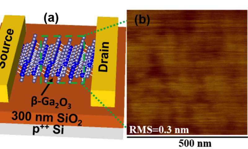
Some researchers have already demonstrated the extreme performance potential of the experimental transistor that is made by a semiconductor, which is called the beta gallium oxide. This experimental transistor is able to bring some new super-efficient switches, which could be applied in some important areas, such as; military ships, aircraft and most importantly in various power grids.

This semiconductor is now being considered as the promise for the “power electronics” of the next generation. It is also promises of developing devices, which can be used in controlling the flow of the electrical energies in respective circuits. It can be noted that this kind of  power electronics technology is able to help in reducing the use of the global energy and also the emission of the greenhouse gas, just by replacing the heavy duty power electronic less efficient switches, which are now used in different facilities.

The specific transistor, known as a gallium oxide on an insulator field effect transistor, called GOOI, which is specifically promising as it is possessing an “ultra-wide bandgap”; the trait that is needed for switches, used in applications of high-voltage. Very recently, these power electronics findings are being stated in details in the research paper, published in the IEEE Electron Device Letters. Hong Zhou, one of the Graduate students, has performed the major parts of this research.

Conclusion

According to the Peide Ye, the Richard J and Mary Jo Schwartz professor of the electrical and engineering division of the internationally acclaimed Purdue University; devices made from the beta gallium oxide is far more superior, compared to other semiconductors, which are promising for specific transistors. The beta gallium oxide is having a higher degree of “breakdown voltage; the point of voltage, where the failure occurred in devices. The research team has also developed the maiden cheaper method by using adhesive tapes to separate layers of the specific semiconductor from the single crystal.


read more
Technology News

Your Android Device Pattern Lock can be Cracked Within Five Attempts

Your Android Device Pattern Lock can be Cracked Within Five Attempts

People make use of the pattern lock in order to secure their Android devices against the unwanted access. You would be surprised by more than 40 per cent makes use of pattern lock on their smartphone and tablets a while rest makes use of either PIN codes, text passwords or doesn’t even to set up a lock system.

Once a pattern lock has been activated on a smartphone or tablet then have to draw their pattern on the on-screen grid of dots to complete the same pattern in order to gain access to their device content. When this pattern matches with the preloaded pattern as done by the users previously then device is unlocked for normal usage. The only hitch is that the system offers only five attempts to get the right combination in place before device for good. But some researchers at the Lancaster University has  come up with an innovative way which helps in cracking the super secure pattern lock with awesome accuracy.

People behind this discovery

The team researchers had come together from Northwest University in China, Lancaster University as well as University of Bath together. They had shown their research where simply using the video and computer vision based algorithm software they were able to crack the Pattern lock. Researchers simply took the video of users drawing the pattern lock but without seeing the screen and the software helped in coming with the right pattern lock by simply analyzing it.

During their research more than 120 unique patterns were collected from the independent users and their software has been to crack almost 95 per cent of patterns within the five attempts. So if this software lands in the hand of the attackers then will be able to figure out the targeted individuals’ pattern with great ease and simplicity.

Complex pattern are hard to crack is a misconception

Most of the people wrongs held the notion that having complex patterns for performing the financial transaction from smartphone or tablet is a secure way. But during their research they found that the complex patterns was quite easier to crack but the shorter and simpler patterns are more secure as it takes more time to figure them with accuracy. If you wish to protect the sensitive information, then stop using complex passwords on your device.

Researchers even put forward list of countermeasures to prevent any kind of attack on your device. First make sure you fully cover the fingers while drawing the patterns. Secondly opt for dual unlocking features which include not just drawing the pattern but also entering the sentence as it happens with Swype.

If you can get your device change the screen color and brightness while drawing the pattern then it will help in confusing the recording to a great extent. The complete finding of this research will be presented at The Network and Distributed System Security Symposium 2017 which is notable conference on cybersecurity.

read more
Technology News

Terahertz Chips a New Way of Seeing through Matter

Terahertz Chips a New Way of Seeing through MatterChips a New Way of Seeing through Matter

How often a day passes with no technological news and no discovery to ease our lives? Hardly a day in this digital era. There have been recent reports from the famous researchers of Princeton University that now they have designed microchips which are capable of transmitting as well as receiving the terahertz waves. Well, it is surely has created a wave among the other scientists as well.

THE WAVE

The terahertz wave is a particular wave, which lasts one millionth of a millionth of a second. It has some unique features as well which will surely blow your mind when you come to know about them. It can penetrate the non-conductive materials which is quite beneficial for the medical purposes as well as when it comes to the security measures in airport like screening and all. The wave is often considered, difficult to use; as it requires a huge amount of terahertz generators and lasers.

THE CHIP

The researchers have designed a unique and most probably a game changing chip of the era. With the collaboration of hard work from the researchers in Princeton University, the terahertz make an interaction with the chip which ultimately leads to a different magnetic field. The rest is then done by the researchers. They deduce the patterns formed by the waves, which help them to conclude. When innovation and thinking out of the box are the keys to define things now, then the scientists also follow the same path. They have now been successful in formulating huge amount of terahertz wave pulses and also combining them. Well, a fact that needs to be known is that currently the chip is operating on the lower part of the wave band. In future, they are planning to expand it. The work is still going on.

THE SECOND CHIP

Well, a second chip has been designed to capture and read the details of the waves. The system is same as that is designed for the smart phones and other gadgets. The cost is moderate ranging to a few dollars.

THE PROPERTIES OF THE WAVE

Being a part of the EM spectrum, it also includes X-rays and visible light. Having less energy than the X-rays, they do not harm the tissues or the DNA of humans. With the ability to interact with chemicals, they can be used in spectroscopy as well. The development is promising and the work is still in progress. The design is just like a big puzzle and perhaps this is the first one. With much work required to expand the along the terahertz band, we have to wait until the final chip comes out in the market. The researchers are confident that they would come out with the solution of mixing the waves on the chip. For time being, the patience is the key factor for the normal netizens like us and hope that the work is done in the most efficient manner.

read more
Technology News

Who is Liable for George Hotz Self Driving Software?

Who is Liable for George Hotz Self Driving Software?

Open Source Self Driving Software Becomes a Liability For The Users

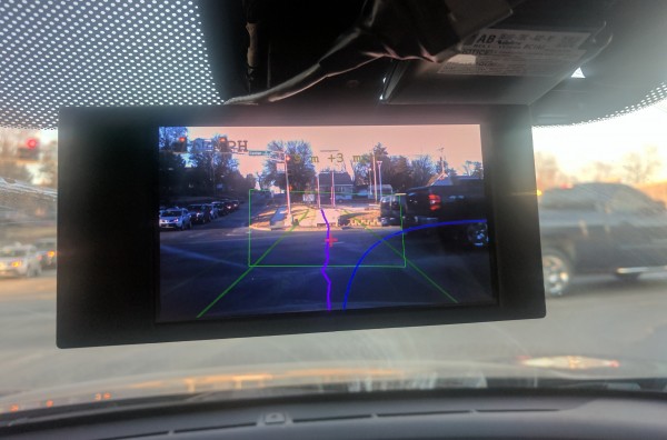
If you are eagerly waiting for the self driving vehicles to launch in upcoming years so you could enjoy the ride in a much enhanced fashion then you wouldn’t have to wait that long. You can go the Comma.ai website and download the open source Python code from the Github. This code along with some necessary hardware adjustment along with following the strict instructions guidelines forwarded by the site will help in turning specific models of Acura and Honda model cars into autonomous vehicles.

The best thing about the open source code offered by Comman.ai is that it comes with much needed safety features. But the major issue which has emerged from this code is that if it suffers from a bug and leads to crashing of the car either into the building, another vehicle or even a pedestrian then who would be held responsible

Self Driving_2

Comman.ai Puts Its Hand in the Air

Comma.ai CEO George Hotz has clarified that the self driving code given by the site is not his own and website has simply released it but it will keep maintaining it. Legal experts believe that making use of this code in the modern cars isn’t wrong and if something goes wrong then it is the users who is to be blamed. But on other hands the Consumer Watchdog advocate going by the name John Simpson finds this stance completely unfair for the users.

He explains that the company has to be held responsible for mishaps which occur due to the shortcoming of the software. Even one can’t point the fingers on the company which has released the source code into the wild because it is open source and with time more number of developers will come forward to modify the code. It would be great if both the company and users is held liable for the unwanted actions purported by the users due to the problems associated with the software at any given point.

Self Driving_1

Laws On Autonomous Self Driving Vehicles Are Still Being Shaped

Comma.ai has opened a can of worms which was being avoided by the major car manufacturer for quite some time. Tesla, Apple and Google are the front runner in developing the autonomous self driving car which will be making way within half a decade but there is no set of rules still in place for them. Autonomous driving legislation is still shaping up all around the world. Some of the automobile manufacturing has already put their step forward in taking all the responsibility in case something goes wrong in their self driving software. Tesla and Volvo have done taken responsibility for their technology in a bid to infuse trust in their upcoming self driving vehicles.

There had already been lawsuits filed against the open source codes finding its way into the commercial products. Having open source code in any commercial consumer product is a nightmare as it leads to forming of vulnerability and backdoor for exploits which can be harmful or works against the consumers.

read more
Technology News

Researchers Create Synthetic Skin

Researchers Create Synthetic Skin

We have all heard of skin grafting and how invaluable it has proved in treating burn patients. However recent researchers at Stanford have shown that it is possible after all to lead science in a direction to create synthetic skin. The research was carried on extensively in the Stanford university in California and was published on the 17th of November after two whole years. What the researchers claimed to find was simple: they were searching for alternative materials which could be wearable and could potentially imitate the properties of skin, especially its healing properties as responsiveness to touch.

The research team at Stanford has, for the first time in the history of mankind has found that the electric properties of the organic semiconductors could be amalgamated with the self healing properties and potentialities of skin along with the flexibility in the area of stretching that is unique to human skin. While skin grafting depends on taking your own and replacing it on the damaged surfaces, this research, which was also assisted by the Dr. Bob C. Schroeder, is actually focused on a brand new sort of polymer which has properties of semi-conduction. While most mind may wonder how this could be done, the mechanism or the prototype of it seems to be devilishly simple.

The polymer of synthetic skin construct is dual layered: the first layer comprising, the sensing mechanism and the bottom layer is in charge of transmitting the signals which translate them into a stimulus of the biochemical nature which is compatible with the nerve cells. The top layer of the synthetic skin also happens to have a peculiarly powerful sensor which much like the actual human skin can feel the pressure from the same range. For example, if you are shaking hands with someone who actually has the prototype synthetic skin, they would feel the same stimulations upon a handshake or a even a simple finger tap perhaps on the shoulder.

The prototype synthetic skin has been made to suffer mechanically induced injuries and has proven capable of sustaining and triumphing over those just like original human skin. However if there is one thing that is still plaguing the minds of the researchers, is how they could make the product with lesser toxic solvents and what more could be improved in the field of self healing.

At the initial stages of the synthetic skin research, the team had found that the rubbers and plastics can be used as sensors of pressure and their molecular structures can be tested for flexibility and springiness. The natural sensitivity of this polymer was then utilised to aid in the conduction of electricity by squeezing the nano tubes of the plastic together. This in turn helps the plastic sensor to emulate human skin. And the brain receives the signals as transmissions of short electrical pulses. The more the pressure on the nano tube the more the varied impulses. Once the impulse is completely stopped, the pulses relax, the feeling produced due to this is akin to a gentle touch. This pressure sensing mechanism was later used for the second ply of their synthetic skin, which could even impart the electricity of the skin cells.

If everything goes smoothly, medical science could potentially be giving back life to a lot of patients!

read more
Technology News

Data Skin: New Soft Electronics Fabrication Method is a Step toward DIY Smart Tattoos

Data Skin: New Soft Electronics Fabrication Method is a Step toward DIY Smart Tattoos

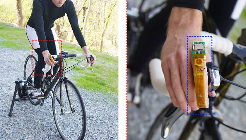
A Mechanical Engineering Professor Carmel Majidi from Carnegie Mellon University, Eric Markvicka a Ph.D. student and former postdoctoral fellow MichaelBarlett have formulated an innovative method that can develop electronics based on your skin’s sensitivity that too very quickly and in a cost-effective way called Data Skin. This is an electronic device that can be worn, much similar to a fitbit that will cling like a tattoo or a sticker that is capable of reading your pulse and can effectively take into notice all the gestures of your hand.

The whole idea seems very tempting and appealing, but such electronic gadgets are based on your skin’s sensitivity is also subjective to several challenges.

The technology included in this device is interfaced with circuits which are very soft along with some microchips that rigid in nature and requires electrical hardware which should be capable for apprehending, processing and analyzing power.

The Mechanical engineering professor said that this electronic hybridity leads to several kinds of breakthrough relating to fabrication of digital techniques that supports the entire process of effective manufacturing of electronics that would be both wireless and soft including other properties like water-resistance, and adhesives which are based on medical grades.

The electronics which are developed from this method contains such vital components which are extremely rigid which is generally found on circuit boards, like transistors, microprocessors and power regulators that fall in the category of those electronics which are based on a circuit board.

This electrical gadget sustains wires which are soft and deformed which supports stretching as well as bending.

This data skin method is most commonly found in those commercial films which is responsible for the creation of those electronics with the help of fast prototypes and assembled techniques.

The team of Engineers, professors and fellows has successfully lead to the formulation of entirely functional data based skin called data skin under the speculation of an hour. The method is based on those tools and materials which are extremely inexpensive and the circuits which are to be used can be produced with the help of not even a dollar.

When it would be folded around the tip of your finger, the data skin which wrapped by an optical pulse based oximetry chip that is capable checking heart rates and generation of oxygen in your blood and can get clubbed to the back portion of your hand so that is can measure your hand gestures.

After being used your data skin can be peeled of easily without any sort of pain and then you can finally discard it. Since, the whole process of manufacturing is very fast and cost-effective, data skin enables the users to formulate the extremely customized data that can be worn on skins.

This is very big step in towards such a big innovation that supports fabrication of the data as per your preference that too without being aided by any experts. The whole creation process lies in your grip and you can create the data based wearables that suits your skin.

read more
Technology News

Engineers Create Room Temperature Multiferroic Material

Engineers Create Room Temperature Multiferroic Material

Creation Of Multiferroic Material In Room Temperature

Researchers in the Department of Materials science and engineering at Cornell University witnessed the creation of Multiferroic Material in room temperature for the first time in the history of science. We are talking about the year 2014, when a group of scholars published their work, a paper on Multiferroics, which is the only known material which is both ferroelectric and magnetic and hence magnetism can be controlled in room temperature. All you need to do is apply an electric field at room temperature.

At first, we try to know a bit regarding multiferroic material and how it works.

What Do You Mean By Multiferroic?

Multiferroic are materials which are both ferroelectric as well as magnetic. There are very few ferroelectrics which have magnetic properties and so it is difficult to create. Moreover, in most of the Multiferroic created, the properties are fully expressed in low temperatures. This the reason why this particular paper is very important because for the first time, Multiferroic was known to work in room temperature.

Researchers Involved In The Whole Process:

The researchers were as follows:

  • Darrell Schlom- Herbert Fisk Professor of Industrial Chemistry in the Department of Materials Science and Engineering.
  • Dan Ralph- F.R. Newman Professor in the College of Arts and Sciences.
  • Ramamoorthy Ramesh- Professor at UC Berkeley.

David Muller and Craig Fennie assisted this group headed by Professor Schlom. They both are professors of applied Engineering and physics. Both of them have partnered the group to generate a new Multiferroic at room temperature by combining two non-Multiferroic materials.

The paper, “Atomically engineered ferroic layers yield a room-temperature magnetoelectric Multiferroic” was published on 22nd of September, authors of which are Julia Mundy along with Muller and Schlom, Charles Brooks and Megan Holtz.

About The Research:

The researchers planned in combining two materials to create the Multiferroic material in room temperature.

  • Ferrimagnetic Oxide (LuFe2O4) – This comprises of alternating monolayers of Lutetium oxide with double mono layers of iron oxide.
  • Hexagonal lutetium iron oxide (LuFeO3) – it comprises of alternating single mono layers of iron oxide and lutetium oxide.

The former is ferroelectric but not magnetic whereas the latter is a strong ferrimagnetic oxide.

After combining both of these, they just added another iron oxide monolayer to each ten atomic recurrences of LuFeO3 and hence they got exactly what they needed.

Infrastructural benefits of Multiferroic:

All the research and experiments were done in the Schlom Lab. The lab, known for its infrastructure made the work very easy for the professors. The material hence made was tested at the Lawrence Berkeley National Laboratory (LBNL) and it was proved that the material actually expressed the desired properties at area temperature.

Ferromagnetism is really important for their revocable polarization and the fact that they can hold this polarization without being connected to power. The project was very successful and was funded by a number of universities and institutes including collaborations from University of Illinois, National University of Standards and Technology, the University of Michigan, Penn State University and funds from U.S. Department of Energy’s Office of Basic Energy Sciences, Division of Material Science and Engineering.

read more
Technology News

New Plastic Material Begins to Oscillate Spontaneously in Sunlight

no thumb

Scientists Discover New Plastic That Oscillate Under Sunlight

Materials that move under light have been known to mankind for years. But this light had to be ultraviolet light for the desired effect to take place. In a path-breaking research, scientists from Eindhoven and Berlin have developed a new plastic substance that freely oscillates when kept directly under the rays of the sun. This is a brilliant new development as intense ultraviolet rays could damage the material itself. Now, the same behavior is being exhibited under visible, unfiltered daylight.

Description of the Plastic Material

Researchers from Eindhoven University of Technology and Humboldt University in Germany have presented this discovery in a journal titled ‘Nature Communications’. They developed new plastic which is made of a polymer layer containing photo-sensitive molecules, also known as ‘azo-dyes’. When placed under sunlight, the thin film starts to spontaneously and irregularly move by itself. The pliable new plastic thus has a self-cleaning surface and can be used to develop a variety of things like solar cells, for example.

Reasons for this Mysterious Behavior

Scientists have not been able to completely explain the cause behind this behavior of the new plastic yet. Michael Debije suggests that it could be because of a combination of factors. The light sensitive molecules of the new plastic display a tendency to bend, stretch and shift their positions when kept under the influence of direct unprocessed daylight. Now, these molecules are bound together like a series within a larger polymer network of crystals.

Once the photo-sensitivity of the cells are activated under visible light, they exhibit behavior similar to getting cramped. This results in the oscillating movement as displayed by the plastic strip. Because of this, the final result is one of a self-oscillating strip of polymer actuator which when driven by sunlight displays chaotic behavior. The researchers have concluded that there is a lot more to this tiny discovery which can only be known through further research.


Benefits from this New Find

This discovery could be revolutionary as a self-cleaning material. The oscillating polymer can be used as a self-cleaning surface. According to researcher Debije, surfaces that are constantly moving by itself will also keep itself clean. It would be very difficult for sand, dust and other environmental agents to get stuck to a constantly vibrating surface. Therefore, this new plastic can be used to build self cleaning solar panels in inaccessible areas like deserts where both water supply and human intervention is scarce as well as inconvenient.

This idea has been put forward by fellow researcher Dick Broer. But this is only the tip of an iceberg. Scientists believe that this principle can be applied to a whole range of different things. Debije believes that this is just the beginning and there could be a bright future lying ahead of the self oscillating plastic. A lot more research is necessary to know the unknown and the researchers hope to attract the attention of many more fellow researchers from all across the globe.

read more
1 18 19 20
Page 20 of 20